

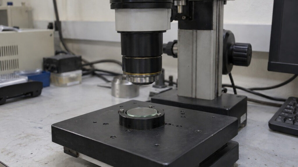
In precision photonics, the performance of a complete system depends on the quality of every optical component. Small surface defects, contamination, and coating irregularities can compromise the intended optical response. Recent research is making inspection more sensitive to defects that are difficult to distinguish in transparent parts. A 2026 study by Ke and colleagues combines controlled illumination, image preprocessing, and an edge-based AI system to detect subtle defects in transparent molded optical components [1]. Such work illustrates how component validation can benefit from developing the imaging setup and the analysis method together.
Recent advances also connect defect detection with measurement and physical behaviour. Huang and colleagues (2025) combine dark-field imaging, image segmentation, and geometric measurement to estimate defect dimensions on planar optical components [2]. Their approach addresses an important distinction: locating an imperfection is only the first step toward deciding whether it is acceptable. In a September 2026 study, Zhang and colleagues combine bright- and dark-field imaging, photothermal absorption characterization, and infrared thermography to investigate scratches on K9 glass [3]. This multimodal approach links visible surface features with thermal response, providing information that an inspection image alone cannot supply.
At Photonics International R&D center, we validate components against the systems they will enter. Our work includes checking UV-C filters for both useful transmission and very low out-of-band leakage, and characterising input windows across the 200 nm–1.1 µm range covered by our sensor roadmap. For demanding solar-blind applications, the target may require unwanted transmission at the 10⁻⁶ level; demonstrating this requires careful control of stray light and the instrument noise floor. Coatings intended for defence hardware undergo environmental sequences before optical retesting measures any degradation. We connect measured deviations to their expected system-level effects, so that component data can guide acceptance, redesign, or further testing.
The next step is to make validation more repeatable across component geometries and production conditions. Research published in 2026 addresses automated centering and annular scanning for inspecting large-aperture curved optics [4], extending inspection beyond flat samples. At our Center, this supports a development direction toward automated inspection and AI-assisted evaluation alongside calibrated measurements. Before transferring a method into production, we need to establish its detection limits, measurement uncertainty, and performance on representative components. Results from a particular research dataset do not by themselves establish acceptance criteria for another product. The aim is to connect recent inspection advances with traceable evidence of readiness for the intended system.
REFERENCES
[1] Ke, K.-C., Chu, Y.-H., & Lin, Y.-H. (2026). Real-time edge AI inspection for subtle defects in transparent optical components. Advances in Mechanical Engineering, 18(5). https://doi.org/10.1177/16878132261449101https://dodmrl.com/MRL_Deskbook_2022__20221001_Final.pdf
[2] Huang, J., Zhang, W., Jin, W., & Hu, H. (2025). Surface defect size measurement of planar optical components based on image segmentation. Optics & Laser Technology, 187, Article 112818. https://doi.org/10.1016/j.optlastec.2025.112818https://cordis.europa.eu/project/id/101213727
[3] Zhang, F., Zheng, J., Wang, Z., Wang, S., Li, X., Huang, S., Guo, J., Li, L., Tao, W., Cui, H., Hai, K., Zang, Z., & Liu, D. (2026). Photothermal response and temperature distribution of surface defect on optical components. Applied Optics, 65(26), 9177–9185. https://doi.org/10.1364/AO.605736https://www.photonics21.org/download/ppp-services/photonics-downloads/Photonics_Strategic_Research_and_Innovation_Agenda_2028-2034_C1.pdf
[4] Zhang, F., Wang, Z., Wang, S., Huang, S., Li, X., Lv, X., Guo, J., Li, L., Hai, K., Zang, Z., & Liu, D. (2026). Automated centering and annular scanning strategy for surface defect detection of large-aperture curved optical components. Optics & Laser Technology, 200, Article 115147. https://doi.org/10.1016/j.optlastec.2026.115147